


All electronic devices we use today ranging from cell phones, TV, computers, smart speakers, have one thing in common in their manufacturing process namely Silicon Wafer.
Silicon wafers are thin slices of pure crystalized silicon. These pure forms of wafers are normally called undoped or intrinsic silicon wafer. One of the reasons for using Silicon wafer in semiconductor industry is the natural abundance of Silicon. It is one of the most abundant material found on earth usually found in the form of SiO2. Another reason of using silicon is that electrical characteristics of the silicon can be precisely controlled by addition of dopants. Silicon wafers that are doped with impurities such as Boron create P- type wafers and wafers that are doped with Arsenic or Phosphorous create N-type wafers. The P type wafers have several positive charged holes whereas N type wafers have several negative charged electrons in it.
If we look at the history of manufacturing of electronic devices/components, the very first electronic devices were mainly based on vacuum tubes. They were used mainly for switching and amplification, just like transistors. However vacuum tubes were inefficient and bulky. In 1956 a solid-state transistor was invented in Bell Labs. It was made of Germanium and was used as electrical amplifier. These solid-state transistors were used building devices such as diodes, capacitors and resistors. All these electronics components were manufactured as discrete devices and electrical connection between these devices were made with wires.
The first Integrated Circuit (IC) happened when all these discrete components were manufactured in same wafer. This was done in 1959 by Jack Kilby at Texas Instruments. It was based on Germanium. In his integrated circuit he had transistors, diodes, capacitors and resistor. However modern integrated circuit based on silicon was developed by Robert Noyce while working at Fairchild camera. The advantage of using silicon was that Si02 layer can be easily used as insulating/dielectric layer to create MOSFET. He also used evaporated Aluminum to create electrical connections instead of wire and thus a true integrated circuit was created, more commonly called as monolithic IC as of today. Monolithic => all electronic components on same wafer.
Over the decades, two types of improvements have been seen in IC manufacturing. The first one is process improvement where manufacturing is done with smaller dimensions. This is sometimes referred to as feature size or node capability of the fabrication lab (10nm, 7nm, 5nm). Over the years, this has reduced from several um (micrometer) to few nm (nanometer) now. Another type of improvement is structural improvement. This essentially means we have new types of devices to make ICs for higher performance. For example, original architecture of transistor was planar which is now replaced tri-gate architecture which provides wider channel and thus provides better current capabilities.
In addition to this, the size of the silicon wafers has increased (from 50mm in 1970s to 300mm as of today) to allow denser and very large integration (VLSI). The increasing wafer size lowers the cost of the chips/circuits to be made but this comes at cost of rebuilding the fabrication lab to handle bigger wafers.
The process of IC manufacturing can be broadly categorized as
- Material preparation – sand to poly Silicon
- Wafer preparation – poly Silicon to Silicon wafer
- Wafer fabrication and sorting of integrated circuits
- Packaging
- Electrical testing
The first two steps are mainly outside the fabrication lab and we will concentrate for that in this article.
The IC fabrication needs a pure (impurity level of less than 1 ppb) single crystal Silicon wafer to manufacture ICs. Silicon wafer are usually classified as Si (100) or Si (111). This allows the identification of the wafers easier within the fabrication lab.
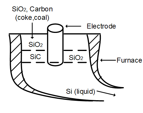
The starting point for the wafer manufacturing is Silicon in form of SiO2 or quartzite. This quartzite is somewhat pure form Silicon but still include metallic impurities. So, first step is reduction of this SiO2 to get pure Silicon. For this quartzite is mixed with Carbon in the form of coke and this process is taken in a submerged electrode arc furnace.
SiC + SiO2 ——-> Si + SiO + CO
The temperature of the process is high enough to get Silicon in molten form which is separated easily. This Silicon, normally referred as metallurgical grade silicon, is 98% pure form of Silicon with minor Aluminum and Iron impurities.
Figure 1: Metallurgical Grade Silicon Extraction
Next step is to purify this extracted silicon using fractional distillation process. Here Silicon is reacted with Hydrochloric gas in a reactor at around 300 celcius
Si + 3HCl ——-> SiHCl3 + H2
The SiHCl3 gas is separated by fractional distillation and then reduced using hydrogen gas.
2SiHCl3 + 2H2 ——-> 2Si + 6HCl
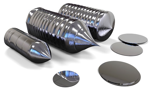
The above process can be repeated several times to get a more purified form of silicon, normally referred as Electronic grade silicon. The electronics grade silicon is still a poly crystalline silicon rather than single crystal of Silicon. So next step is to convert this extracted silicon into a single crystal wafer.
One of the methods to make a single crystal silicon out of poly crystalline silicon is called Czochralski growth method. This process is most dominant method and used to create 80-90% of the wafers used in the fabrication lab. In this process the pure silicon is molten first in a furnace. The furnace is heated using RF heated coils at around 1500 degrees. Then a seed crystal with right orientation is taken and is put on the rotor. The seed silicon is dipped into the molten silicon and slowly withdrawn with a rotation. With the process of withdrawing the seed crystal, molten silicon gets attached to the seed silicon and takes the same orientation as seed crystal as soon as it cools down. The rotation is done in conjunction to the withdrawal process to create a uniform piece of cylindrical silicon.
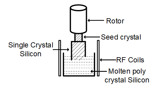
Figure 2: Czochralski Method
The created Single crystal silicon needs shaping and cutting process. For this process an industrial diamond is used. The seed is removed from the generated single crystal Silicon and surface grinding is done to increase the smoothness. After the surface griding, flats are grinded on the silicon. The flats are ground along the lengths of the wafers. The flats can be Primary flat or Secondary flat. The flats are related to crystal orientation and used for identification and sorting purposes.
Different silicon wafers are grounded different flats. For example, a P type wafer with orientation of 111 has only one primary flat, where as a N type wafer with orientation of 111 has one primary and one secondary flat. Similarly, P[100] and N[100], both have primary as well as secondary flats but with different angles to each other.
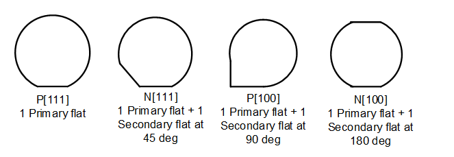
Figure 3: Silicon Wafer Flat Types
After the grounding, the silicon is then cut to create silicon wafer. Again, an industrial grade diamond is used for wafer slicing. After that, the created wafers are passed through a chemical etching process to remove any damage as well as contaminated region on the wafers. Later, these wafers are passed through a polishing step. The polishing can be single side, or double sided but single sided polishing is more common. Once polished these wafers are ready to be used in the fabrication lab.
Bạn Có Đam Mê Với Vi Mạch hay Nhúng - Bạn Muốn Trau Dồi Thêm Kĩ Năng
Mong Muốn Có Thêm Cơ Hội Trong Công Việc
Và Trở Thành Một Người Có Giá Trị Hơn
Bạn Chưa Biết Phương Thức Nào Nhanh Chóng Để Đạt Được Chúng
Hãy Để Chúng Tôi Hỗ Trợ Cho Bạn. SEMICON