 PCB Designer
Applied Micro Circuits Corporation
Lot D.01, Tan Thuan Street, Tan Thuan Export Processing Zone, Tan Thuan Dong Ward, Dist 7, HCMC
Applied Micro Circuits Corporation, or AppliedMicro, is an innovator in semiconductor technology and a global leader in energy efficient sustainable solutions to process, transport, and store information for next generation Internet data center and telecommunication carrier central office equipment. As a leader in high-speed digital signal, Internet Protocol, Ethernet packet and storage processing, AppliedMicro’s patented innovations provide highly integrated Systems-On-a-Chip (SoCs) for telecommunications, enterprise and consumer applications.
AppliedMicro’s corporate headquarters are located in Sunnyvale, California USA. Sales and Engineering offices are located throughout the world.
AppliedMicro Vietnam provides very good benefit programs and working conditions:
- Competitive 13 month salary + performance bonus
- 15 annual leave days per year
- Professional working environment
- Flexible working hour
- Personal Healthcare Insurance for employee and family
- Personal Accident Insurance for employee and family
- International Travel Insurance
- Petrol and home ADSL Allowance
- Daily lunch provided
- Opportunities to travel and work overseas such as USA, Japan, India, China, Taiwan, etc.
- And other benefit programs will be informed in the new hire orientation section
Company website: http://www.apm.com
Please forward resumes to Địa chỉ email này đã được bảo vệ từ spam bots, bạn cần kích hoạt Javascript để xem nó.
Company size: 100-499
Work Location: Ho Chi Minh
Job Level: Experienced (Non-Manager)
Job Category: Electrical/Electronics
High Technology
Telecommunications
Preferred Language: English
PCB Designer
Job Description
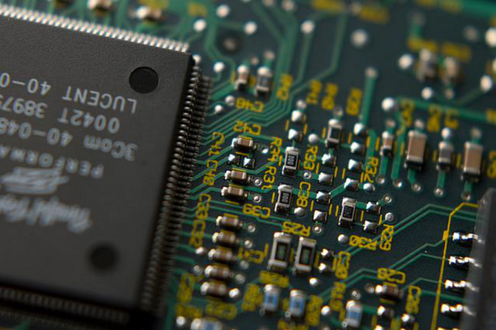
As a PCB Designer, your primary responsibility involves performing component placement and routing Multi-Layer Printed Circuit Boards using Allegro and PADS tools.
You will also be responsible for developing Allegro and PADS footprints and maintain standard symbol libraries for AppliedMicro hardware engineering teams, both in Ho Chi Minh City and in the US.
Responsibilities
· Work with a team of engineers to perform component placement and Multi-Layer PCB routing.
· Building and maintaining an Allegro Library database, creating component footprints, and generating schematic symbols.
Qualifications
· 2+ years of PCB layout experience.
· Experience with Cadence Allegro PCB tool.
· Experience in all aspects of PCB design: footprinting, netlisting, constraint setup, placement, routing, and generating gerbers.
· General understanding of electronic circuits and chip functionality.
· Able to read and understand schematics
· Good English communications skills, both verbal and writing.
· 2 years Technical College or Vocational training in electronics and PCB design.
Location
AppliedMicro Design Center in Ho Chi Minh City, Vietnam.