


Noise Margin
Gate circuits are constructed to sustain variations in input and output voltage levels. Variations are usually the result of several different factors.
- drop
- High operating temperatures may cause a drift in transistor voltage and current characteristics
- Spurious pulses may be introduced on signal lines by normal surges of current in neighbouring supply lines.All these undesirable voltage variations that are superimposed on normal operating voltage levels are called noise. All gates are designed to tolerate a certain amount of noise on their input and output ports. The maximum noise voltage level that is tolerated by a gate is called noise margin. It derives from I/P-O/P voltage characteristic, measured under different operating conditions. It's normally supplied from manufacturer in the gate documentation.
- LNM (Low noise margin): The largest noise amplitude that is guaranteed not to change the output voltage level when superimposed on the input voltage of the logic gate (when this voltage is in the LOW interval). LNM=VILmax-VOLmax.
- HNM (High noise margin): The largest noise amplitude that is guaranteed not to change the output voltage level if superimposed on the input voltage of the logic gate (when this voltage is in the HIGH interval). HNM=VOHmin-VIHmin
tr (Rise time)
The time required for the output voltage to increase from VILmax to VIHmin.
tf (Fall time)
The time required for the output voltage to decrease from VIHmin to VILmax.
tp (Propagation delay)
The time between the logic transition on an input and the corresponding logic transition on the output of the logic gate. The propagation delay is measured at midpoints.
Power Dissipation.
Each gate is connected to a power supply VCC (VDD in the case of CMOS). It draws a certain amount of current during its operation. Since each gate can be in a High, Transition or Low state, there are three different currents drawn from power supply.
- ICCH: Current drawn during HIGH state.
- ICCT: Current drawn during HIGH to LOW, LOW to HIGH transition.
- ICCL: Current drawn during LOW state.For TTL, ICCT the transition current is negligible, in comparison to ICCH and ICCL. If we assume that ICCH and ICCL are equal then,
Average Power Dissipation = Vcc * (ICCH + ICCL)/2
For CMOS, ICCH and ICCL current is negligible, in comparison to ICCT. So the Average power dissipation is calculated as below.
Average Power Dissipation = Vcc * ICCT.
So for TTL like logics family, power dissipation does not depend on frequency of operation, and for CMOS the power dissipation depends on the operation frequency.
Power Dissipation is an important metric for two reasons. The amount of current and power available in a battery is nearly constant. Power dissipation of a circuit or system defines battery life: the greater the power dissipation, the shorter the battery life. Power dissipation is proportional to the heat generated by the chip or system; excessive heat dissipation may increase operating temperature and cause gate circuitry to drift out of its normal operating range; will cause gates to generate improper output values. Thus power dissipation of any gate implementation must be kept as low as possible.
Moreover, power dissipation can be classified into Static power dissipation and Dynamic power dissipation.
- Ps (Static Power Dissipation): Power consumed when the output or input are not changing or rather when clock is turned off. Normally static power dissipation is caused by leakage current. (As we reduce the transistor size, i.e. below 90nm, leakage current could be as high as 40% of total power dissipation).
- Pd (Dynamic Power Dissipation): Power consumed during output and input transitions. So we can say Pd is the actual power consumed i.e. the power consumed by transistors + leakage current.Thus
Total power dissipation = static power dissipation + dynamic power dissipation
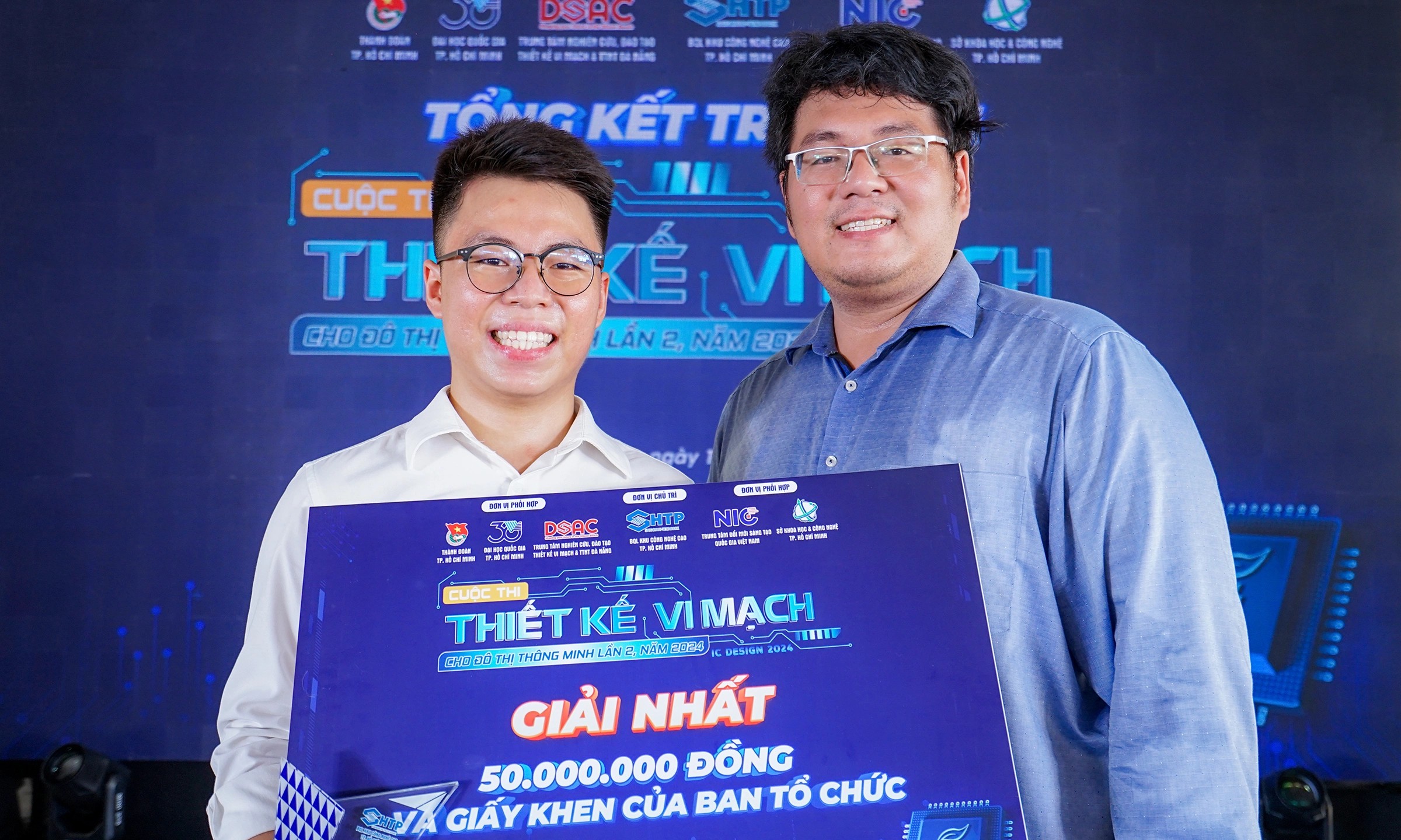
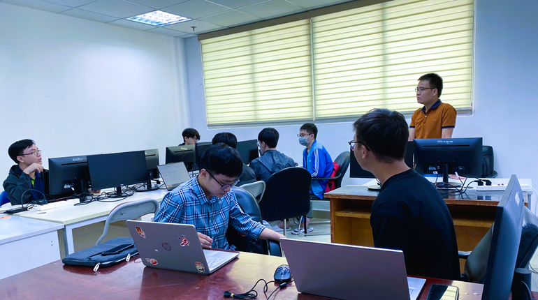
Bạn Có Đam Mê Với Vi Mạch hay Nhúng - Bạn Muốn Trau Dồi Thêm Kĩ Năng
Mong Muốn Có Thêm Cơ Hội Trong Công Việc
Và Trở Thành Một Người Có Giá Trị Hơn
Mong Muốn Có Thêm Cơ Hội Trong Công Việc
Và Trở Thành Một Người Có Giá Trị Hơn
Bạn Chưa Biết Phương Thức Nào Nhanh Chóng Để Đạt Được Chúng
Hãy Để Chúng Tôi Hỗ Trợ Cho Bạn. SEMICON